The increasing complexity of advanced semiconductors is creating a manufacturing challenge that cannot be resolved through improvements in production equipment alone. As chip designs become more intricate, the computing resources required to prepare them for manufacturing are becoming a potential constraint on production efficiency and technological progress.
Siemens and NVIDIA are addressing this problem through an expanded collaboration that uses GPU acceleration to reduce the time required for computational lithography, a critical stage in semiconductor manufacturing.
By integrating NVIDIA’s cuLitho technology with Siemens’ Calibre manufacturing software, the companies have achieved simulation speed improvements of at least tenfold, with verified results ranging from 10 to 17 times faster across key workloads. Full-chip optical proximity correction operations can be accelerated by up to 12 times.
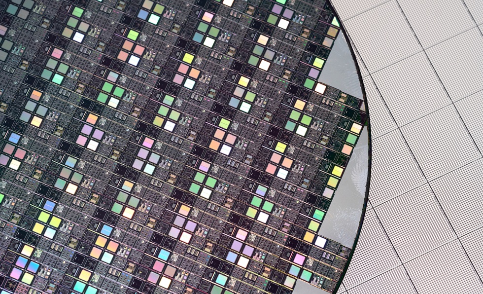
Computational lithography is used to optimise the patterns transferred onto semiconductor wafers during manufacturing. As chip features become smaller and more complex, manufacturers must account for distortions that can occur during the lithographic process, requiring extensive simulation and adjustment before production begins.
These demands are becoming more pronounced with the introduction of High Numerical Aperture Extreme Ultraviolet lithography, known as High-NA EUV, and advanced patterning techniques such as inverse lithography technology.
Although these methods can improve patterning precision, their computational requirements have historically restricted how extensively they can be applied across entire chip designs. Engineering teams have consequently faced compromises between the depth of optimisation and the time available before manufacturing.
The Siemens and NVIDIA collaboration is intended to reduce these constraints by accelerating simulation and enabling more comprehensive optimisation of photomasks used in semiconductor production.
Faster processing allows engineers to evaluate additional design iterations and identify potential lithographic hotspots before tapeout, the stage at which a chip design is finalised for manufacturing. Identifying these problems earlier can improve process margins and reduce risks affecting manufacturing yield.
The implications extend to the production of AI processors and advanced memory devices, where increasingly complex designs are placing additional pressure on manufacturing processes.
For semiconductor manufacturers, the development demonstrates how computing infrastructure is becoming an increasingly important element of production technology. Improvements in manufacturing capability depend not only on the precision of physical equipment but also on the speed and sophistication of the software used to prepare and optimise production processes.
GPU acceleration potentially changes the economics of computationally intensive manufacturing workflows by making techniques previously constrained by processing time more practical at full-chip scale.
As semiconductor complexity continues to increase, the ability to simulate and optimise manufacturing processes efficiently could become a determining factor in how quickly advanced chip designs can move from engineering development into production.